291 Minibyte CPU
291 : Minibyte CPU
- Author: Zach Frazee
- Description: A super simple 8-bit CPU
- GitHub repository
- Clock: 50000000 Hz
How it works
The Minibyte CPU is a simple "toy" 8-bit CPU that uses a custom RISC instruction set
The CPU also has some built in DFT (Design For Test) features and a Demo ROM that can be enabled for easy testing (some external hardware required)
This was created mostly as a learning/reference project to get more familiar with Verilog
Specs
Max CLK Frequency: 50Mhz (untested)

Data Buss Width:    8 bits
Address Buss Width: 8 bits (only 7 bits usable due to limited IO)

Registers:
    A   - 8 bits wide - Accumulator
    M   - 8 bits wide - Memory Address Pointer
    PC  - 8 bits wide - Program Counter
    IR  - 8 bits wide - Instruction Register
    CCR - 2 bits wide - Condition Code Register

Memory Mapped Registers:
    R0  - 8 bits wide - Gen Purpose Reg 0
    R1  - 8 bits wide - Gen Purpose Reg 1
    R2  - 8 bits wide - Gen Purpose Reg 2
    R3  - 8 bits wide - Gen Purpose Reg 3
    R4  - 8 bits wide - Gen Purpose Reg 4
    R5  - 8 bits wide - Gen Purpose Reg 5
    R6  - 8 bits wide - Gen Purpose Reg 6
    R7  - 8 bits wide - Gen Purpose Reg 7

Number of Instructions: 37

ALU:
    Data Inputs: 2x 8 bit inputs
    Data Output: 8 bits (result) + 2 bits (flags)

    Operations Supported:
        PASSA - Passthrough input A
        PASSB - Passthrough input B
        ADD   - Add A and B
        SUB   - Subtract B from A
        AND   - Logical and of A, B
        OR    - Logical or of A, B
        XOR   - Logical xor of A, B
        LSL   - Logical shift A left by B
        LSR   - Logical shift A right by B
        ASL   - Arithmetic shift A left by B
        ASR   - Arithmetic shift A right by B
        RSL   - Rotary shift A left by B
        RSR   - Rotary shift A right by B

    Flags:
        Z - Set if result is 0, otherwise clear
        N - Set if result is a negative signed int, otherwise clear
Pinout
uio[7:0]    - DATA IN/OUT BUSS
ui_in[7:0]  - DFT Test and Configuration Select
uo_out[7]   - WE (Write Enable Signal)
uo_out[6:0] - ADDR OUT BUSS
Architecture
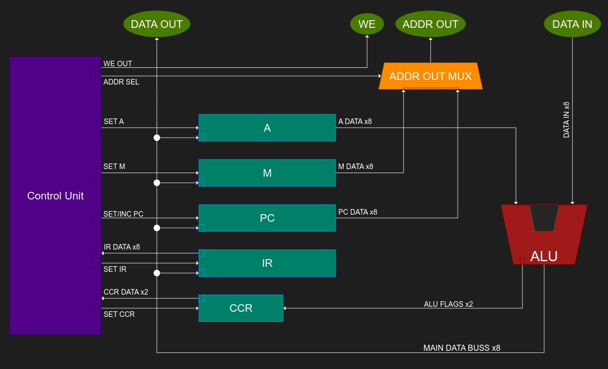
The Minibyte CPU uses a very traditional architecture where most data is manipulated via a single accumulator (A Register)
The ALU operates on data from the A Register and either direct data (from memory indexed by the M register), or immediate data (from the current instruction's operand indexed by the PC register)

*Note that DFT and testing features are not represented in the above block diagram
Power Up State
Upon reset, the device will be initialized with all registers cleared to 0x00. This includes the program counter (PC register). It is expected that the program memory will start at address 0x00 to begin execution.
Instruction Set
The Minibyte CPU has 4 instruction format types. The program memory is chunked into bytes. Some instructions only occupy a single byte, while others occupy 2 bytes for an opcode and a following operand
| Type | Length | Desc |
|---|---|---|
| Inherent | 8 - bits | IR with no operand |
| Immediate | 16 - bits | IR with an operand containing DATA |
| Direct | 16 - bits | IR with an operand containing an ADDRESS |
| Indirect | 16 - bits | IR with an operand containing an ADDRESS that points to another ADDRESS |
As a visual reference, here is how we would expect a basic program to be structured in memory. Please note that all programs start execution from address 0x00 as shown.

The above program adds the numbers 0x05 and 0x03 together, and then loops back to the starting IP of 0x00
Inherent IR:
| Type | OP[7:0] |
|---|---|
| Inherent | IR OPCODE |
Immediate/Direct IR:
| Type | OP[15:8] | OP[7:0] |
|---|---|---|
| Immediate | IR OPCODE | OPERAND DATA |
| Direct | IR OPCODE | OPERAND ADDRESS |
| Indirect | IR OPCODE | OPERAND ADDRESS |
Opcode Table:
| OPCODE | HEX | Operand | CCR |
|---|---|---|---|
| NOP | 0x00 | N/A | N/A |
| LDA_IMM | 0x01 | Immediate | N/A |
| LDA_DIR | 0x02 | Direct | N/A |
| STA_DIR | 0x03 | Direct | N/A |
| STA_IND | 0x04 | Indirect | N/A |
| ADD_IMM | 0x05 | Immediate | N/A |
| ADD_DIR | 0x06 | Direct | N/A |
| SUB_IMM | 0x07 | Immediate | N/A |
| SUB_DIR | 0x08 | Direct | N/A |
| AND_IMM | 0x09 | Immediate | N/A |
| AND_DIR | 0x0A | Direct | N/A |
| OR_IMM | 0x0B | Immediate | N/A |
| OR_DIR | 0x0C | Direct | N/A |
| XOR_IMM | 0x0D | Immediate | N/A |
| XOR_DIR | 0x0E | Direct | N/A |
| LSL_IMM | 0x0F | Immediate | N/A |
| LSL_DIR | 0x10 | Direct | N/A |
| LSR_IMM | 0x11 | Immediate | N/A |
| LSR_DIR | 0x12 | Direct | N/A |
| ASL_IMM | 0x13 | Immediate | N/A |
| ASL_DIR | 0x14 | Direct | N/A |
| ASR_IMM | 0x15 | Immediate | N/A |
| ASR_DIR | 0x16 | Direct | N/A |
| RSL_IMM | 0x17 | Immediate | N/A |
| RSL_DIR | 0x18 | Direct | N/A |
| RSR_IMM | 0x19 | Immediate | N/A |
| RSR_DIR | 0x1A | Direct | N/A |
| JMP_DIR | 0x1B | Direct | N/A |
| JMP_IND | 0x1C | Indirect | N/A |
| BNE_DIR | 0x1D | Direct | Z==CLEAR |
| BNE_IND | 0x1E | Indirect | Z==CLEAR |
| BEQ_DIR | 0x1F | Direct | Z==SET |
| BEQ_IND | 0x20 | Indirect | Z==SET |
| BPL_DIR | 0x21 | Direct | N==CLEAR |
| BPL_IND | 0x22 | Indirect | N==CLEAR |
| BMI_DIR | 0x23 | Direct | N==SET |
| BMI_IND | 0x24 | Indirect | N==SET |
| OPCODE | Desc |
|---|---|
| NOP | No Operation |
| LDA_IMM | Load A with immediate operand data |
| LDA_DIR | Load A with the data stored at the operand addr |
| STA_DIR | Store A at the operand addr |
| STA_IND | Store A at the addr contained at the operand addr |
| ADD_IMM | Add the immediate operand data to A |
| ADD_DIR | Add the data stored at the operand addr to A |
| SUB_IMM | Subtract the immediate operand data from A |
| SUB_DIR | Subtract the data stored at the operand addr from A |
| AND_IMM | And the immediate operand data with A |
| AND_DIR | And the data stored at the operand addr with A |
| OR_IMM | Or the immediate operand data with A |
| OR_DIR | Or the data stored at the operand addr with A |
| XOR_IMM | Xor the immediate operand data with A |
| XOR_DIR | Xor the data stored at the operand addr with A |
| LSL_IMM | Logical shift A left by the immediate operand data |
| LSL_DIR | Logical shift A left by the data at the operand addr |
| LSR_IMM | Logical shift A right by the immediate operand data |
| LSR_DIR | Logical shift A right by the data at the operand addr |
| ASL_IMM | Arithmetic shift A left by the immediate operand data |
| ASL_DIR | Arithmetic shift A left by the data at the operand addr |
| ASR_IMM | Arithmetic shift A right by the immediate operand data |
| ASR_DIR | Arithmetic shift A right by the data at the operand addr |
| RSL_IMM | Rotate A left by the immediate operand |
| RSL_DIR | Rotate A left by the data stored at the operand addr |
| RSR_IMM | Rotate A right by the immediate operand data |
| RSR_DIR | Rotate A right by the data stored at the operand addr |
| JMP_DIR | Jump PC to the operand addr |
| JMP_IND | Jump PC to the addr stored at the operand addr |
| BNE_DIR | Jump PC (if Z is clear) to the operand addr |
| BNE_IND | Jump PC (if Z is clear) to the addr stored at the operand addr |
| BEQ_DIR | Jump PC (if Z is set) to the operand addr |
| BEQ_IND | Jump PC (if Z is set) to the addr stored at the operand addr |
| BPL_DIR | Jump PC (if N is clear) to the operand addr |
| BPL_IND | Jump PC (if N is clear) to the addr stored at the operand addr |
| BMI_DIR | Jump PC (if N is set) to the operand addr |
| BMI_IND | Jump PC (if N is set) to the addr stored at the operand addr |
DFT and Extra Features
The Minibyte CPU has a few DFT features that might be useful on live silicon for debug/testing. All DFT functions are enabled by an active high signal on one of the ui_in[7:0] pins (ui_in[7:0] should be tied to zero during normal operation)
| ui_in Bit | Feature |
|---|---|
| ui_in [7] | Enable Memory Mapped Gen Purpose Registers |
| ui_in [6:5] | Unused |
| ui_in [4] | Enable Demo ROM |
| ui_in [3] | Halt Control Unit on Next Fetch |
| ui_in [2:0] | Debug Output Signal Select |
Gen Purpose Registers:
The Gen Purpose Registers are a set of 8 memory mapped general purpose registers that can be accessed at the following addresses as long as ui_in[7] is held high
| Reg Name | Mem Address |
|---|---|
| Register R0 | 0x78 |
| Register R1 | 0x79 |
| Register R2 | 0x7A |
| Register R3 | 0x7B |
| Register R4 | 0x7C |
| Register R5 | 0x7D |
| Register R6 | 0x7E |
| Register R7 | 0x7F |
Debug Out Select:
The CPU has an extra mux between the normal addr out mux and the uo_out pins. To leverage this ui_in[2:0] can be used to select a debug signal to output on the uo_out[6:0] pins in place of the normal address buss
| Debug Out Select | Function |
|---|---|
| ui_in[2:0] = 0b000 | Normal Operation |
| ui_in[2:0] = 0b001 | Output A[6:0] to uo_out[6:0] |
| ui_in[2:0] = 0b010 | Output A[7] to uo_out[0] |
| ui_in[2:0] = 0b011 | Output M[6:0] to uo_out[6:0] |
| ui_in[2:0] = 0b011 | Output PC[6:0] to uo_out[6:0] |
| ui_in[2:0] = 0b011 | Output IR[6:0] to uo_out[6:0] |
| ui_in[2:0] = 0b011 | Output CCR[1:0] to uo_out[1:0] |
| ui_in[2:0] = 0b011 | Output CU_STATE[6:0] to uo_out[6:0] |
How to test
Simulation
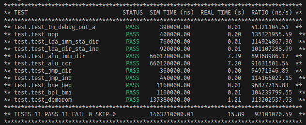
The Minibyte CPU has fairly exhaustive cocotb test suite that is able to test and verify most of the device's intended functionality.
To run the test suite, cd into the ./test directory of the project and run "make"

On Live Silicon
The easiest way to test the Minibyte CPU on live silicon is to use the built-in Demo ROM
To enable the Demo ROM, make sure that ui_in[4] and ui_in[7] are held high on reset, and remain high while the program runs
Holding ui_in[4] high will enable the Demo Rom
Holding ui_in[7] high will enable the General Purpose Registers, which are required/utilized by the Demo ROM program
The Demo ROM will run the following program
PSEUDOCODE:
    WHILE FOREVER{
        //Part 1: Binary Count
        SET A to 0

        WHILE A <= 255 {
            INCREMENT A

            WRITE A to ADDRESS 0x40
        }

        //Part 2: Walking 1
        SET A to 1

        WHILE A > 0 {
            LEFT SHIFT A by 1

            WRITE A to ADDRESS 0x40
        }

        //Part 3: Deadbeef to RAM/Gen Purpose Registers and back out
        LOAD 0xDEADBEEF into R0->R3

        WRITE R0 to ADDRESS 0x40
        WRITE R1 to ADDRESS 0x40
        WRITE R2 to ADDRESS 0x40
        WRITE R3 to ADDRESS 0x40
    }
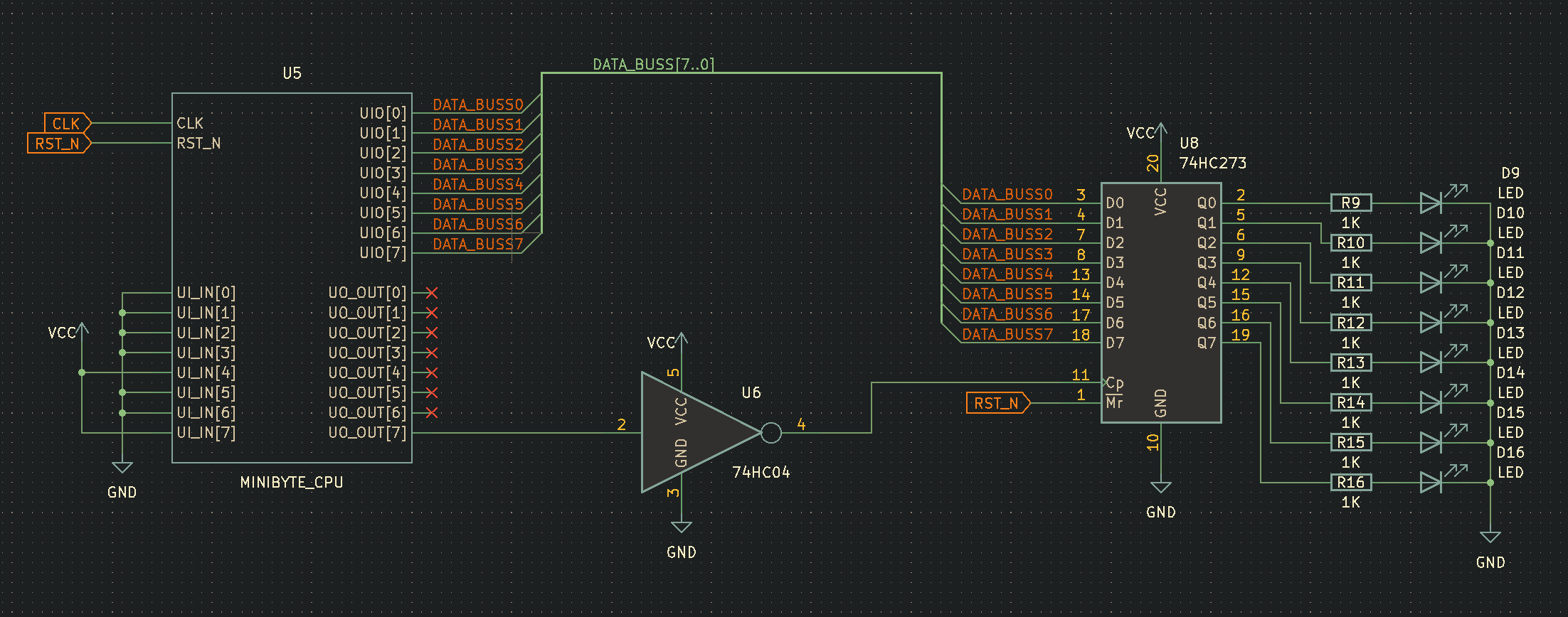
To capture the output of the program with LEDs, it is recommended to add a D-Flip Flop (such as a 74x273 series chip) on the output of the data buss (uio[7:0]). See External Hardware section below for more details
External hardware
Demo Setup

Something similar to the above schematic is recommended when running the Demo ROM. Note that an inverter (such as a 74x04 series chip) should be used as shown on the CLK input of the DFF. We want data to be latched when WE falls to 0 (after the data has had time to set up and make its way out of the chip). Please also note that you will probably need to run the CPU at a fairly low CLK frequency in order to see any LED activity with the naked eye.
Other Setups
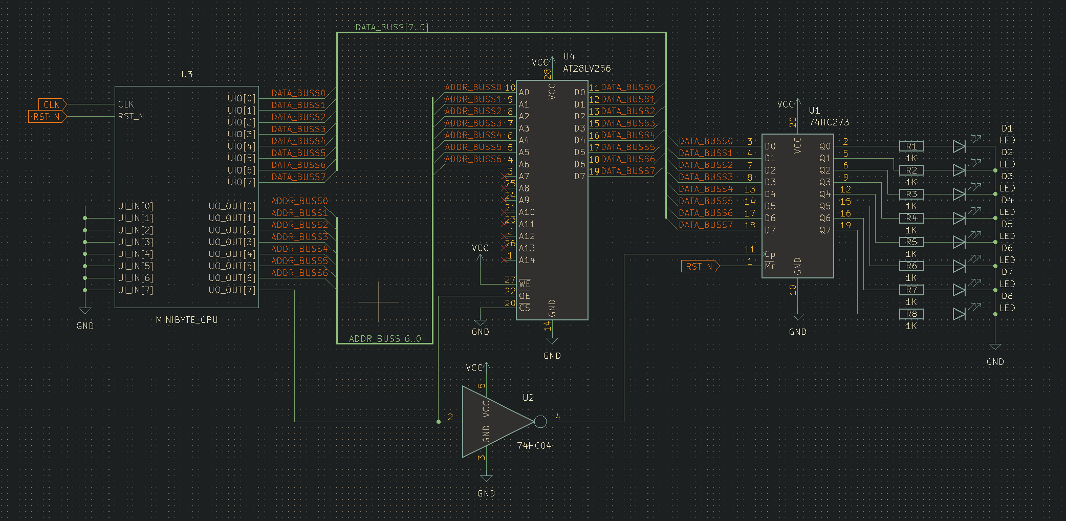
The sky is the limit as far as as what devices you attach to the CPU. If you are writing your own programs, you probably are going to want to attach some sort of external ROM to the main address and data buss. Here is a recommended setup adding an external EEPROM.

Beyond this, you will hopefully find that the Minibyte CPU can be paired with a wide variety 3.3V compatible parallel ROM/EPROM/EEPROM, SRAM, and IO expander modules.
IO
| # | Input | Output | Bidirectional |
|---|---|---|---|
| 0 | DEBUG_OUT_SELECT_0 | ADDR_OUT_0 | DATA_0 |
| 1 | DEBUG_OUT_SELECT_1 | ADDR_OUT_1 | DATA_1 |
| 2 | DEBUG_OUT_SELECT_2 | ADDR_OUT_2 | DATA_2 |
| 3 | HALT_CU | ADDR_OUT_3 | DATA_3 |
| 4 | DEMO_ROM_ENABLE | ADDR_OUT_4 | DATA_4 |
| 5 | ADDR_OUT_5 | DATA_5 | |
| 6 | ADDR_OUT_6 | DATA_6 | |
| 7 | ENABLE_GEN_REGS | WE_OUT | DATA_7 |